
How to Design a USB-C Power Supply (5V–28V) in 3 Hours | Full Tutorial | EasyEDA
1000+ video views
June 8, 2026

Talking About Joulescope Schematic: How Does It Measure Voltage and Current So Precisely?
21366+ video views
May 28, 2026
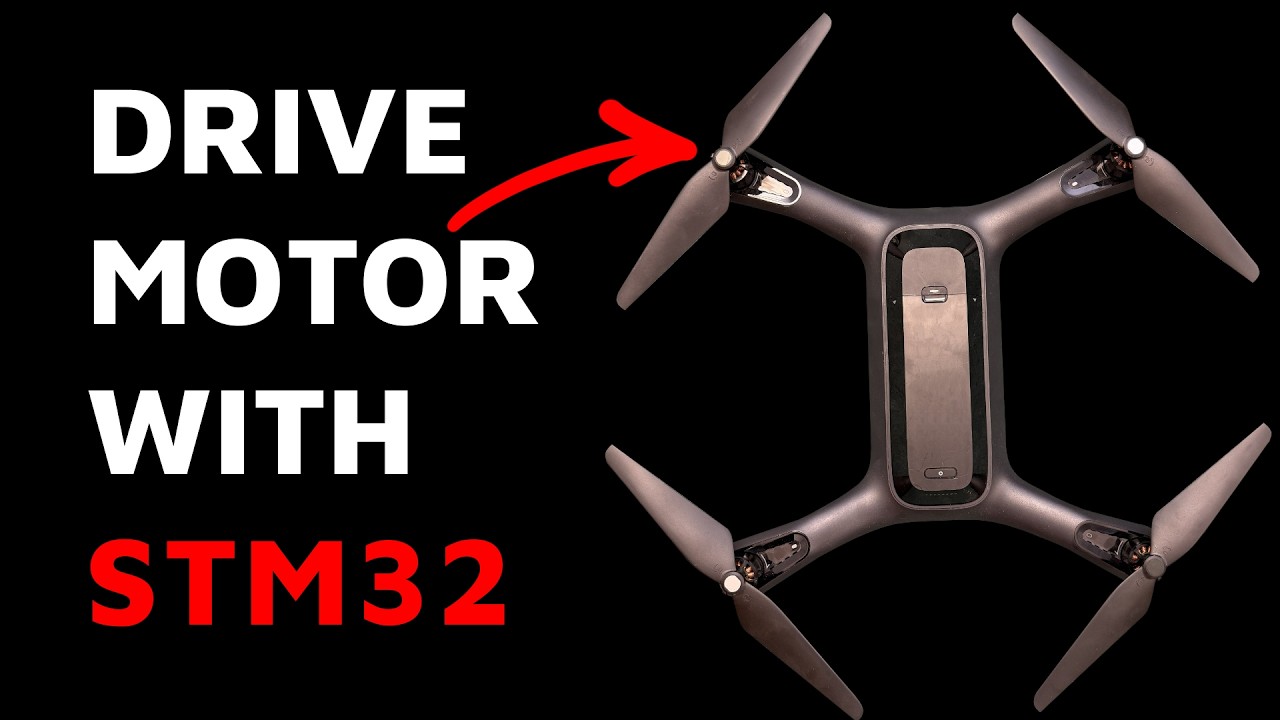
Driving a Motor with STM32 | Quick Tutorial (Drone Example using GaN Controller)
5499+ video views
April 23, 2026
How to Design an Antenna That Actually Works | All Steps Explained
8361+ video views
February 19, 2026
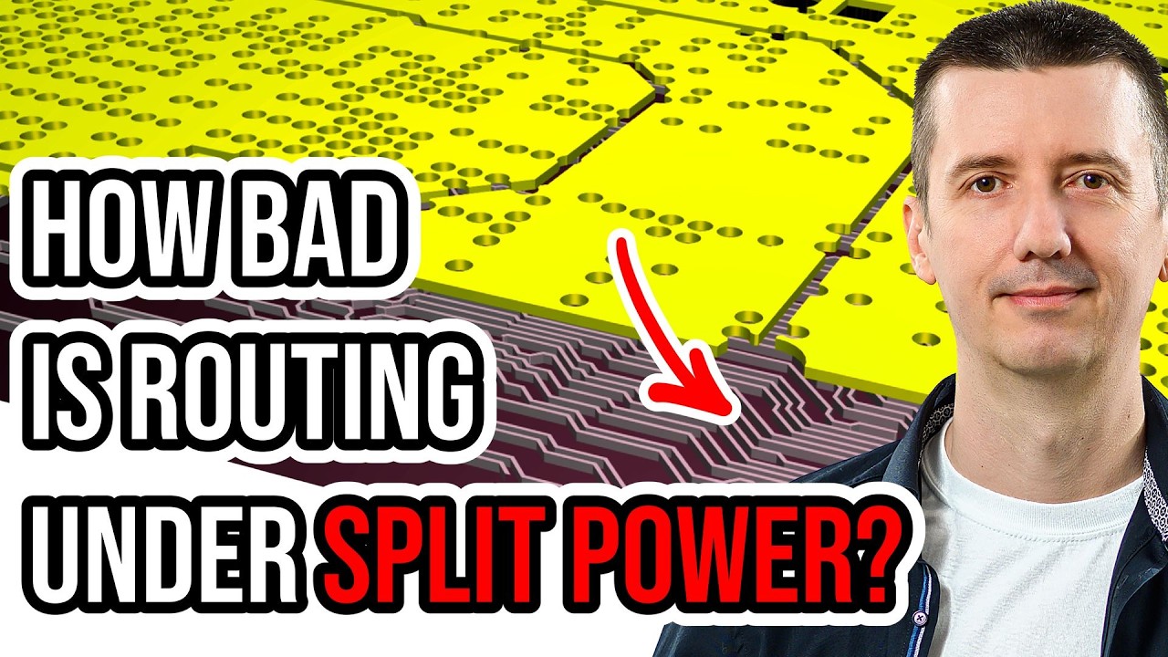
Is this PCB layer stackup OK? Solid GND – Signal Layer – Split Planes
4604+ video views
February 11, 2026
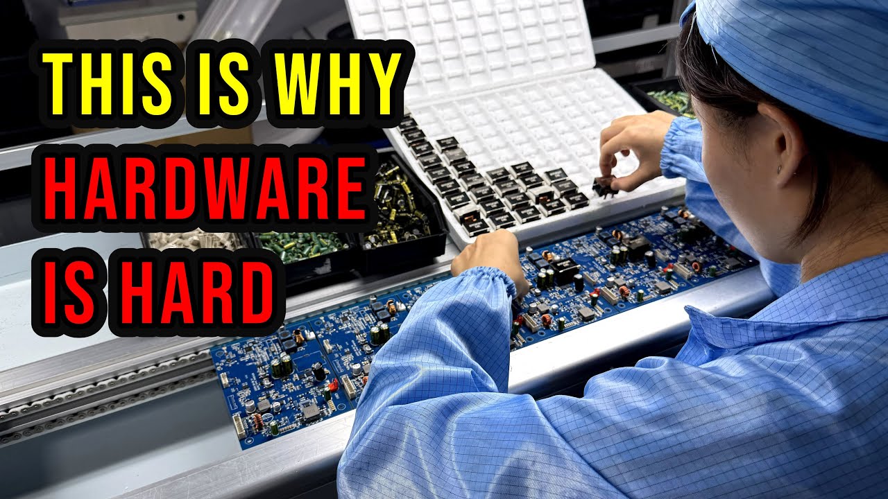
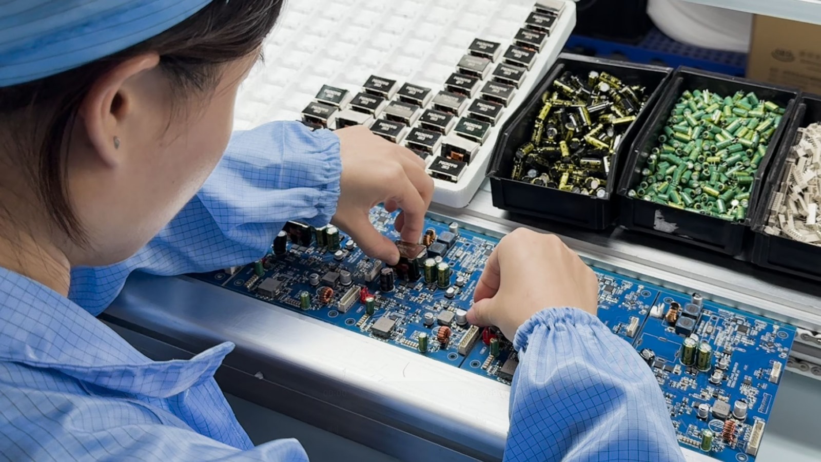
From Idea to Mass Production - Explaining the process of electronic product development
12504+ video views
January 23, 2026
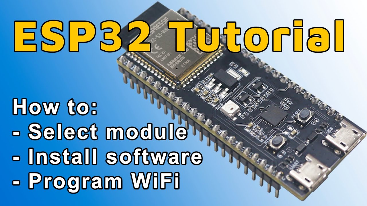
ESP32 for Beginners: Selecting module + Starting with Arduino and Espressif IDE
12745+ video views
November 19, 2025
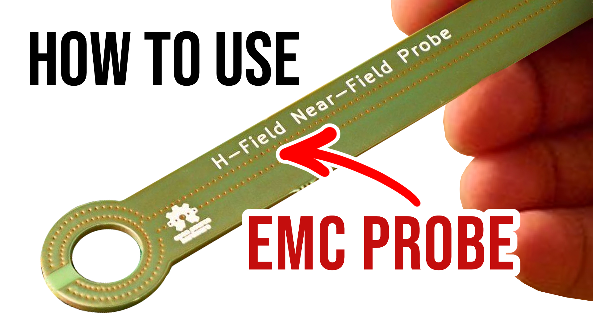
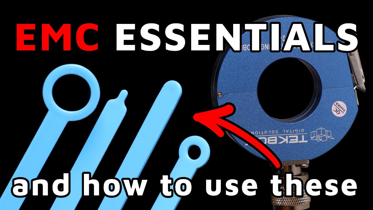
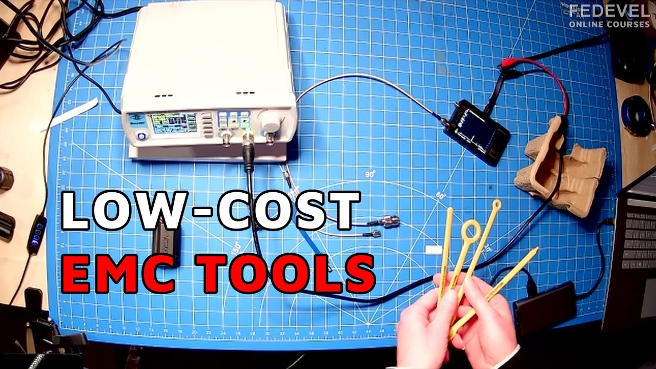
Solving EMC Problems Fast & Easy - Near Field Measurement in Your Lab
7572+ video views
October 30, 2025

Comparing Bluetooth vs. WiFi vs. Cellular - Speed, Distance, Power ...
2998+ video views
September 26, 2025
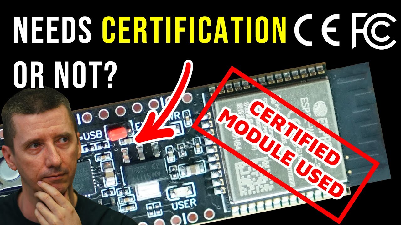
Everyone designing PCB boards needs to watch this - Certification ( FCC & CE )
11018+ video views
September 1, 2025
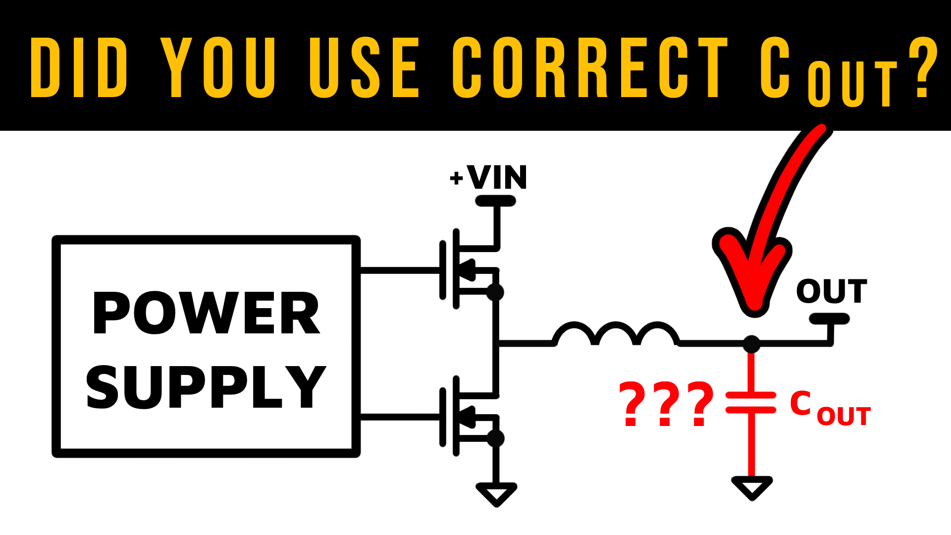
How to Calculate the Output Capacitor for a Switching Power Supply? It's simple. Explained here...
13813+ video views
August 4, 2025


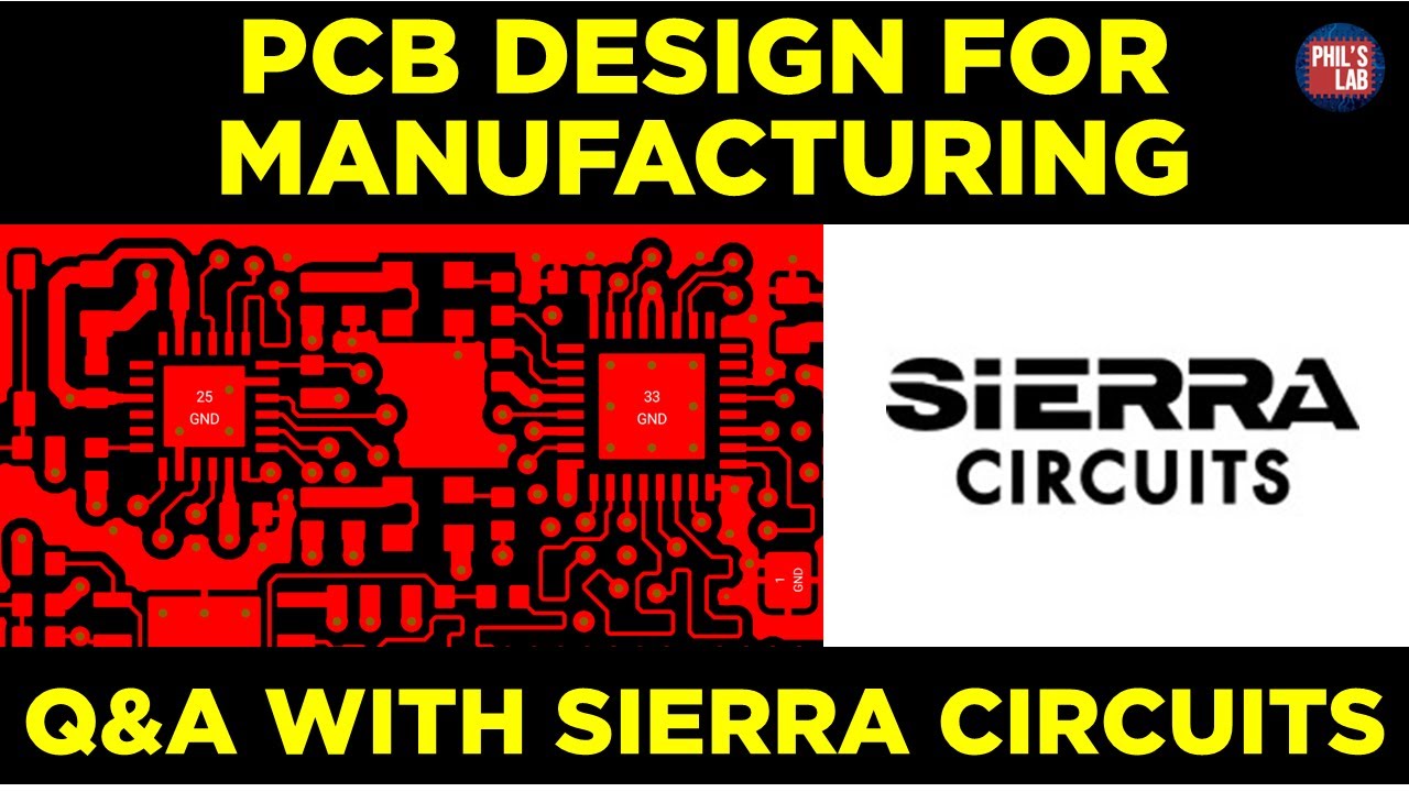
PCB Design for Manufacturing (DFM) Q&A with Sierra Circuits - Phil's Lab #158
12615+ video views
June 17, 2025
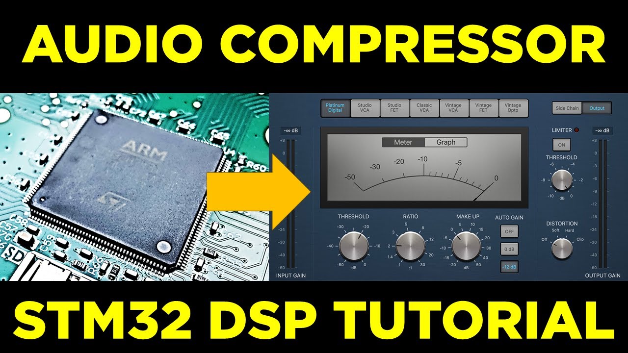
Audio Compressor Software Implementation (STM32 DSP) - Phil's lab #157
12515+ video views
June 8, 2025


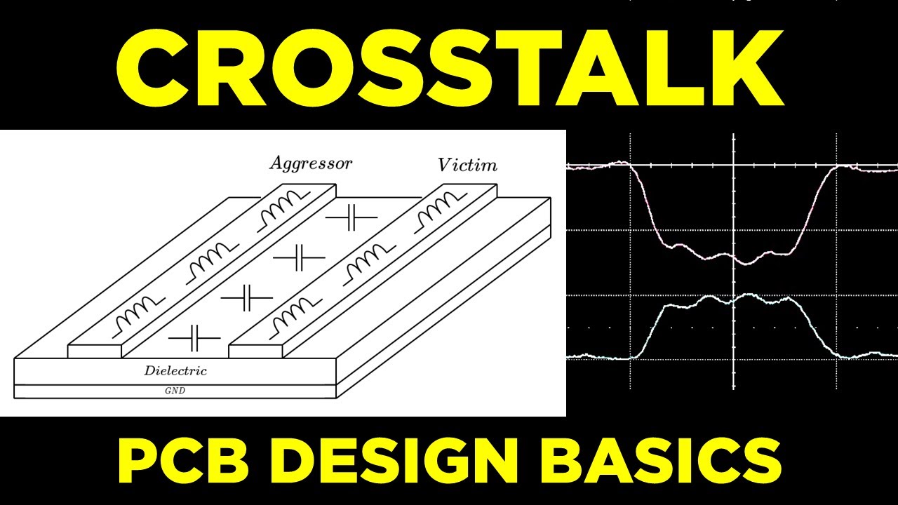


What does an eye diagram show? Here is how you recognize problems - reflections, crosstalk and loss
17704+ video views
April 23, 2025
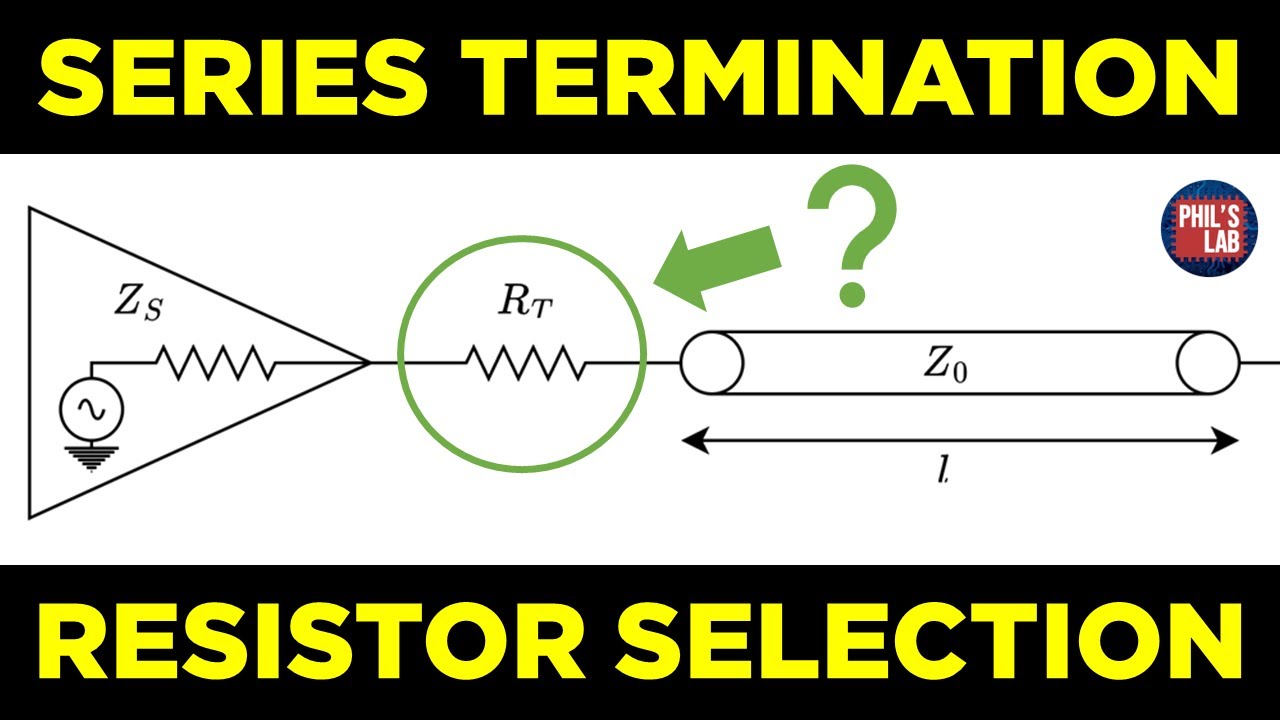
Series Termination Resistor Selection (Practical Demo) - Phil's Lab #155
16039+ video views
April 21, 2025


I built a real electronic product from home… and recorded everything
29708+ video views
March 27, 2025

I asked AI to design an electronic circuit and write software for it. Here is what happened ...
38806+ video views
March 18, 2025

Starting with RP2040 / RP2350 PICO - Programming Tutorial for Beginners | StepByStep | CircuitPython
9588+ video views
March 7, 2025
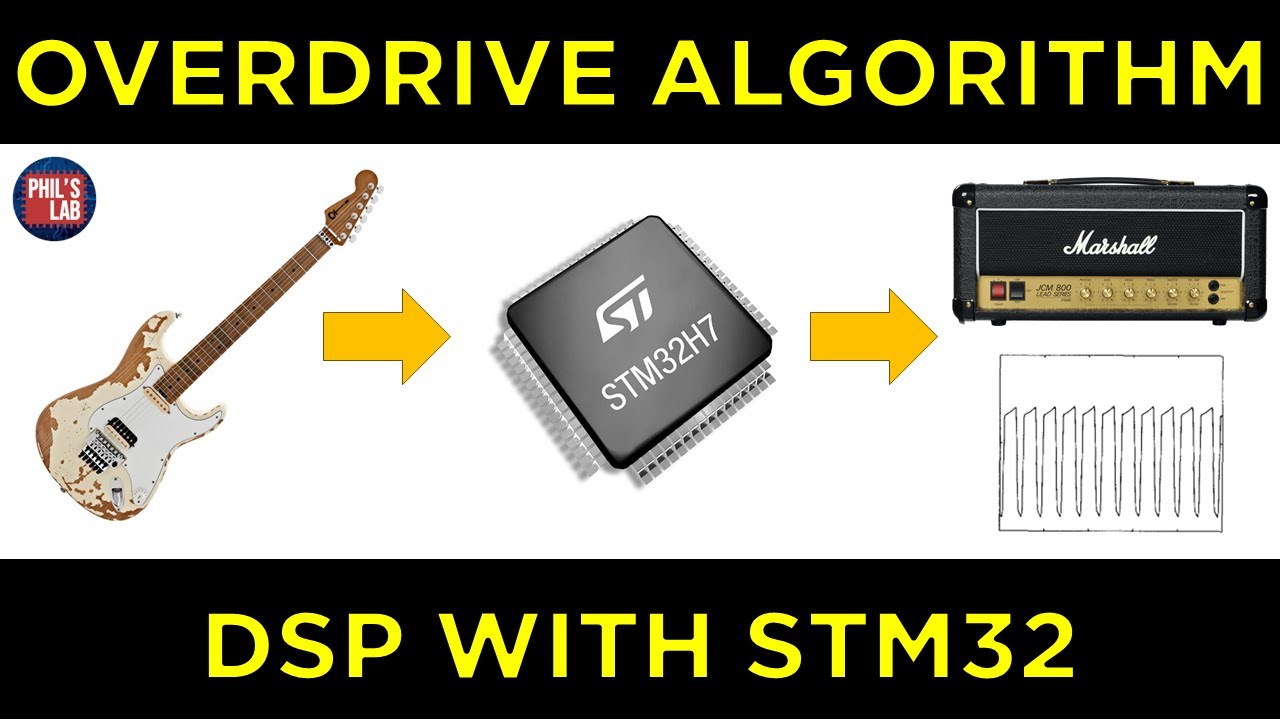
DSP Overdrive (Asymmetrical Clipping) in Software (STM32) - Phil's Lab #153
32218+ video views
February 28, 2025


2-Port Shunt-Through Impedance Measurement Basics - Phil's Lab #151
12372+ video views
January 13, 2025

How to Start with Electronic Circuit Simulation for Free | Eric Bogatin
13817+ video views
January 10, 2025


Capacitor Measurement and Modelling Basics (Bode 100) - Phil's Lab #150
14593+ video views
December 23, 2024


Tutorial - Custom DIY Keyboard Design and Build | Part 7: Manufacturing
5482+ video views
December 3, 2024


Tutorial - Custom DIY Keyboard Design and Build | Part 6: Case / Box design
4953+ video views
November 29, 2024

Tutorial - Custom DIY Keyboard Design and Build | Part 5: PCB Layout Improvement
5556+ video views
November 27, 2024

Tutorial - Custom DIY Keyboard Design and Build | Part 4: PCB Layout
7561+ video views
November 25, 2024

Tutorial - Custom DIY Keyboard Design and Build | Part 3: PCB - Component Placement
7595+ video views
November 20, 2024

Tutorial - Custom DIY Keyboard Design and Build | Part 2: Keyboard Schematic
12964+ video views
November 18, 2024


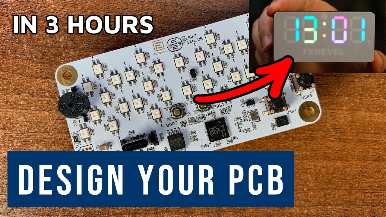
Tutorial - Custom DIY Keyboard Design and Build: Schematic + PCB + Case | Part 1 - RP2040
35786+ video views
November 7, 2024


STM32 Real-Time FIR Filter Implementation (CMSIS DSP) - Phil's Lab #141
23387+ video views
July 22, 2024

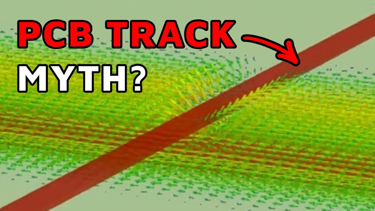
PCB Layout of Differential Pairs vs. Crosstalk - Is track polarity important?
7648+ video views
July 18, 2024

Delay-Based Audio FX Software Implementation (DSP with STM32) - Phil's Lab #140
19255+ video views
July 7, 2024


How To Measure Low Impedance With An Affordable VNA And Using Free Tools
11477+ video views
May 30, 2024


How Much Current Will Destroy a PCB Track? | Track resistance measurements
11424+ video views
May 7, 2024


If your high speed differential pairs don't work, maybe the solution is in software
5816+ video views
March 27, 2024


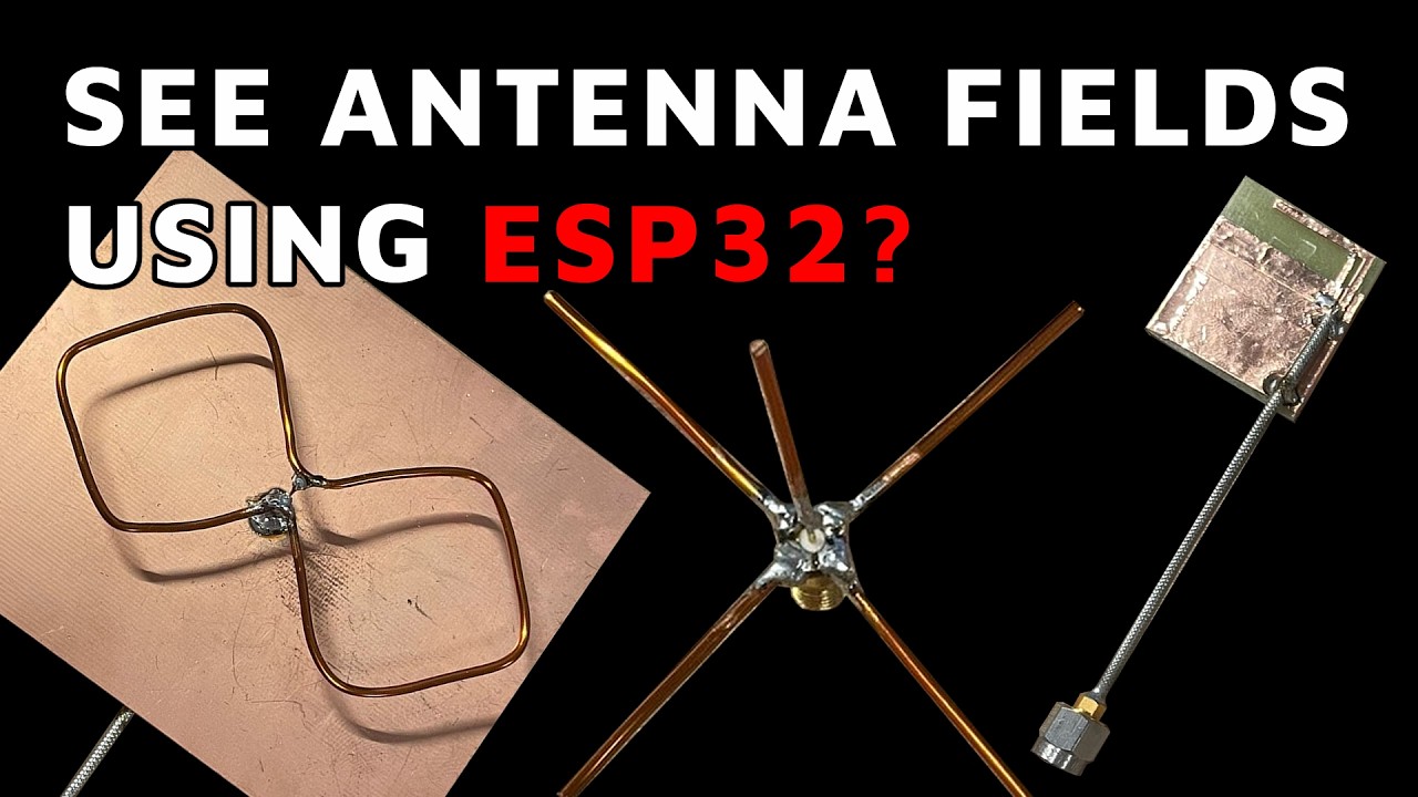
Don't place PCB antenna into middle of your board. Here is why .... | ESP32
20608+ video views
February 21, 2024


QA403 Audio Analyzer Tutorial (Noise, SNR, THD+N, ...) - Phil's Lab #130
16847+ video views
January 31, 2024


Do Differential Pairs Need Ground? Are you sure? | Explained by Eric Bogatin
33853+ video views
January 4, 2024

KiCad 7 STM32 Bluetooth Hardware Design (2/2 PCB) - Phil's Lab #128
245486+ video views
December 22, 2023


KiCad 7 STM32 Bluetooth Hardware Design (1/2 Schematic) - Phil's Lab #127
231277+ video views
December 15, 2023

How to simulate PCIE / IEEE path on PCB + Everything you need to know | Explained by Bert Simonovich
8182+ video views
December 14, 2023

How to probe the silicon inside of a chip | Explained by John McMaster
18068+ video views
December 8, 2023

Real-Time Impulse Response Simulation in Software (STM32 DSP) - Phil's Lab #126
18474+ video views
November 24, 2023

CAN Bus is Simple and Actually Really Cool | Explained by Ken Tindell
37589+ video views
November 16, 2023


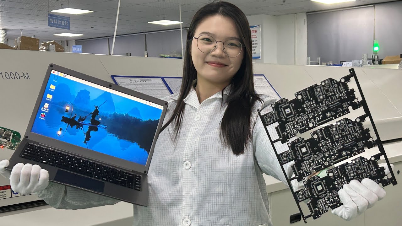
Visiting a Big Factory in China - How they create libraries #EasyEDA #LCSC #JLCPCB
9019+ video views
November 7, 2023

Shall We Use a Ferrite Bead in Power Rail or Not? | Explained by Eric Bogatin
95106+ video views
November 3, 2023

How to Measure And Calculate Board Runtime for a Single Battery Charge - ESP32 Example
11450+ video views
October 27, 2023


Selecting Inductor For Switching Power Supply - Not everyone knows this #HighlightsRF
11887+ video views
September 22, 2023

How PCBs are Manufactured & Assembled (PCBWay Factory Tour) - Phil's Lab #120
36045+ video views
September 18, 2023

Watch How Capacitors Placement Makes a Big Difference #HighlightsRF
20806+ video views
September 14, 2023


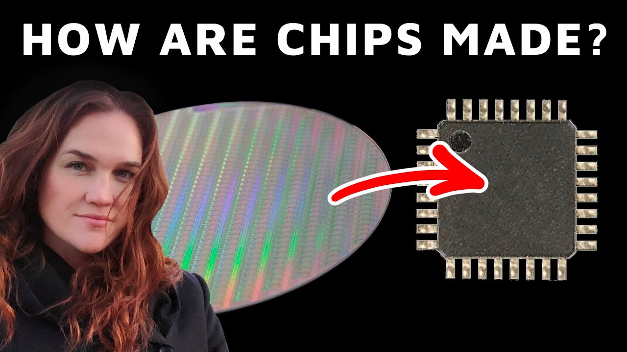
How is a chip (die) connected to the pins? Do you know? #HighlightsRF
8246+ video views
September 7, 2023


Zynq Ultrascale+ Hardware Design (Schematic Overview) - Phil's Lab #116
44052+ video views
July 30, 2023


How To Connect Altium With a Mechanical CAD Software? Here is an example ...
7129+ video views
June 15, 2023


Machine Learning Explained + Example: Arduino and Hand Gesture Recognition | Shawn Hymel
4958+ video views
June 6, 2023

FPGA Design Tutorial (Verilog, Simulation, Implementation) - Phil's Lab #109
126457+ video views
May 31, 2023


Very Important For PCB Layout: Crossing planes explained by Eric Bogatin
15602+ video views
May 16, 2023


Do You Know How Signal Travels Through a VIA? Are You Sure? | Explained by Eric Bogatin
18448+ video views
May 3, 2023


Build Your Own Circuits in Browser | ESP32, Arduino, Raspberry Pi Pico
15840+ video views
April 13, 2023


Hacking Hardware – Ways and tools to find out what an electronic board is doing and influence it
7882+ video views
April 4, 2023


What Decoupling Capacitor Value To Use And Where To Place Them | Eric Bogatin
130364+ video views
February 24, 2023


How to Make Custom Board – Arduino Shield in 2 Hours | Full Tutorial
49996+ video views
February 16, 2023


The Simplest Digital Filter (STM32 Implementation) - Phil's Lab #92
100619+ video views
January 21, 2023

ESP32 Programming Tutorial for Custom Hardware (GPIO, Serial, SPI, WiFi) - Phil's Lab #91
122444+ video views
January 14, 2023


How To Learn PCB Design (My Thoughts, Journey, and Resources) - Phil's Lab #87
334181+ video views
December 17, 2022

How to design perfect switching power supply | Buck regulator explained
83130+ video views
December 8, 2022


When a Signal Hits The End of a PCB Track – What happens? | Reflections by Eric Bogatin
25594+ video views
November 17, 2022

TIP: You can have crosstalk on boards running at low frequency #hw_tip #001
15374+ video views
November 11, 2022

FPGA + PCIe Hardware Accelerator Design Walkthrough (DDR3, M.2, ..) - Phil's Lab #82
204075+ video views
November 4, 2022


Mini 6-Layer Mixed-Signal Hardware Design Walkthrough - Phil's Lab #78
69953+ video views
October 8, 2022

See How Audio Filters Work | Compressor, Notch, Shelf, Limiter and more … | Remco Stoutjesdijk
5280+ video views
October 7, 2022


Must Know This to Understand High Speed PCB Layout Simulation | S-Parameters Explained, Eric Bogatin
18158+ video views
September 23, 2022


How To Promote Your Own Tech Products? | Money, Certification, Marketing
16116+ video views
September 16, 2022


ESD Protection Basics - TVS Diode Selection & Routing - Phil's Lab #75
148868+ video views
September 9, 2022


Extended Kalman Filter Software Implementation - Sensor Fusion #4 - Phil's Lab #73
75872+ video views
August 22, 2022

NOT in the Copper! 3D Animation of a Signal Through a VIA | Yuriy Shlepnev
10947+ video views
August 18, 2022


Unexpected Currents On The Other Side Of GND Plane – You may be surprised | Yuriy Shlepnev
8104+ video views
August 11, 2022


Starting with STM32 – Programming Tutorial for Beginners | Step by Step | Greidi Ajalik
463642+ video views
July 28, 2022

Altitude Estimation with Pressure Sensors (STM32, Firmware + Hardware) - Phil's Lab #68
21135+ video views
July 27, 2022

Cool Projects Explained – FLEX PCBs, Robot, Motors and more | Carl Bugeja
7516+ video views
July 25, 2022


Learn To Fix EMC Problems Easily And In Your Lab – Troubleshooting Immunity Issue | Min Zhang
42603+ video views
July 15, 2022


Which length matching is the best? You may be surprised | Eric Bogatin
44801+ video views
June 30, 2022


Is This The Best Antenna Design And Simulation Software? | Markus Laudien
49037+ video views
June 20, 2022

Things on your boards causing problems during manufacturing | Amit Bahl
8182+ video views
June 16, 2022


Everyone designing boards needs to know this about power and noise | Florian Hämmerle | #HighlightsRF
13741+ video views
May 31, 2022

Altium – How To Do Versioning And Releases | Explained | Michal Faruga
13336+ video views
May 26, 2022

DIY VIA plating - Explained how copper gets inside of a VIA | Kailey Shara | #HighlightsRF
28984+ video views
May 24, 2022


Should you place solder mask over BGA pads? Do you know why? | Tom Hausherr | #HighlightsRF
6408+ video views
May 17, 2022

Do you need thick copper layers in PCB for high currents? Are you sure? | Steve Sandler
43298+ video views
May 12, 2022


PCB Stackup Explained – What layer ordering is good or bad and why | Rick Hartley | #HighlightsRF
36500+ video views
May 10, 2022

Why don’t you measure 50 OHM on a 50 OHM cable? | Eric Bogatin | #HighlightsRF
54746+ video views
May 3, 2022


How to add PCIE to FPGA – Just to give you an idea how it is done | Adam Taylor | #HighlightsRF
17759+ video views
April 26, 2022


Looking at the data inside of a USB signal ( Example: Decoding USB keyboard protocol )
10811+ video views
April 21, 2022


Long vs. Short USB Cable – How much worse the signal looks if a long USB cable is used?
11045+ video views
April 14, 2022


Where To Connect The Shield of a Cable? Explained | Rick Hartley | #Highlights
51971+ video views
April 12, 2022

Is the USB you designed perfect? This is how you test it … | Gregor Hofferbert
12595+ video views
April 7, 2022


STM32 I2S ADC DMA & Double Buffering - Digital Audio Processing with STM32 #4 - Phil's Lab #55
76333+ video views
March 31, 2022

Up to 255 Amps Power Supply Schematic and PCB Layout | Server Board Design | #Highlights
28553+ video views
March 29, 2022

Asking Peter with 100 000+ students: How to Learn Electronics and Programming? | Peter Dalmaris
14501+ video views
March 24, 2022

Do you connect PCB mounting holes correctly? | Keith Armstrong | #Highlights
35080+ video views
March 22, 2022


Tutorial OrCAD 17.4 and Cadence Allegro PCB Editor | 2022 | Step by Step | For Beginners
238318+ video views
March 17, 2022


Altium – Easy Way to Import Schematic Symbol | Part Search | #Highlights
17059+ video views
March 8, 2022

Designing a PCB patch antenna for WiFi and Bluetooth | KiCad | Philip Salmony
73806+ video views
March 3, 2022

Watch How a Few Components Make a Big Difference in EMC/EMI | Min Zhang | #Highlights
38916+ video views
March 1, 2022


Tremolo Effect - Digital Audio Processing with STM32 #3 - Phil's Lab #51
23504+ video views
February 26, 2022

Laser – How does it work? Can you build one at home? | Zachariah Peterson
126833+ video views
February 24, 2022


FPGA & SoC Hardware Design - Xilinx Zynq - Schematic Overview - Phil's Lab #50
83175+ video views
February 21, 2022


Notch Filters - Digital Audio Processing with STM32 #2 - Phil's Lab #49
28296+ video views
February 9, 2022

How to get experience if no one wants to hire you? | Dave Jones EEVBlog | #Highlights
13278+ video views
February 8, 2022


How To Build Your Own Box for a PCB Board (Using Free Fusion 360 Software) – Step By Step Tutorial
73921+ video views
January 27, 2022

What is The Right Pad Shape to use in PCB Footprints? | Tom Hausherr | #Highlights
18180+ video views
January 25, 2022

Digital Audio Processing with STM32 #1 - Introduction and Filters - Phil's Lab #46
150067+ video views
January 22, 2022

Microcontroller in FPGA? This is how to do it … | Step by Step Tutorial | Adam Taylor
74312+ video views
January 20, 2022

Why The VIA Stub Can Make Problems? | Bert Simonovich | #Highlights
15818+ video views
January 18, 2022

Mixed-Signal Hardware Design Overview | Audio SoM | STM32 & Altium - Phil's Lab #45
59850+ video views
January 16, 2022

Every PCB Designer Needs To Know This About PCB Track Impedance | TDR | Eric Bogatin
112721+ video views
January 13, 2022

Course Release - Mixed-Signal Hardware Design with KiCad - Phil's Lab #44
15835+ video views
January 11, 2022

Why is 50 OHM impedance used in PCB Layout? | Explained | Eric Bogatin
150228+ video views
January 6, 2022


Decimation Filters - Theory and Software Implementation - Phil's Lab #42
33567+ video views
December 20, 2021

Making a Magic Wand with Light Effects and Spell Recognition | Wizards Wand
30874+ video views
December 16, 2021

Learn To Fix EMC Problem Easily And In Your Lab – Troubleshooting Radiated Emissions | Min Zhang
97564+ video views
December 9, 2021

STM32 PCB Design - Complete Walkthrough - Altium Designer & JLCPCB - Phil's Lab #41
875041+ video views
December 5, 2021

Many EMC Tips to Help You Design Better PCB Boards (with Keith Armstrong)
69204+ video views
December 2, 2021


Explaining Veritasium Electricity Video: Energy doesn’t flow in wires (with Eric Bogatin)
95597+ video views
November 25, 2021

Notch Filters - Theory and Software Implementation - Phil's Lab #39
31996+ video views
November 21, 2021


Watch a high speed signal travel through your PCB | Simple Animation
32329+ video views
November 11, 2021

Altium STM32 Hardware Design - An Overview in Under 20 Minutes - Phil's Lab #38
46672+ video views
November 11, 2021


How To Design Boards And Electronics for Space (with Cedric Corpa)
18524+ video views
October 21, 2021

Animation, Simulation, Rendering, Movements, Parameters, Constraints (Fusion 360 with Kevin Kennedy)
4374+ video views
October 14, 2021

How To Design a Breakout Board | JLCPCB | Altium Designer - Phil's Lab #35
42235+ video views
October 11, 2021

About HW Engineers, Electronics and Youtube ( with Dave Jones EEVBlog )
40177+ video views
October 7, 2021

How To Build Your Own Box for a PCB Board (Using Free Fusion 360 Software) – Step By Step Tutorial
125303+ video views
September 30, 2021


Accelerometers and Gyroscopes - Sensor Fusion #1 - Phil's Lab #33
130212+ video views
September 25, 2021

Every HW Engineer should know this: Measuring EMC – Conducted Emissions (with Arturo Mediano)
62792+ video views
September 23, 2021

Is Andonstar AD407 PCB / SMT Microscope Good? Image quality is ok (see the video), but the stand ?!
8913+ video views
September 16, 2021

How To Create Difficult FPGA Designs with CPU, MCU, PCIE, ( with Adam Taylor )
157046+ video views
September 9, 2021

IIR Filters - Theory and Implementation (STM32) - Phil's Lab #32
133951+ video views
September 7, 2021

Small Things Damaging Your High Speed Signals (with Bert Simonovich)
18725+ video views
September 2, 2021


9 Simple Tricks to Improve EMC / EMI on Your Boards – Practical examples (with Min Zhang)
157622+ video views
August 19, 2021

Watch How a PCB Layout Change Makes Big Difference – with Eric Bogatin (Ground bounce)
47745+ video views
August 12, 2021


Tutorial #7: How to Write Software And Program Your Board – Step by Step
106495+ video views
July 29, 2021

Raspberry Pi RP2040 Hardware Design | Altium Designer | JLCPCB - Phil's Lab #28
112338+ video views
July 28, 2021

Tutorial #6: Useful Steps To Do After You Receive Your Boards From Production + Some soldering tips
57866+ video views
July 15, 2021

Easy Way to Desolder and Remove Through Hole Connectors or Components
566779+ video views
July 12, 2021

PCB Layout – Useful Calculations Which You Maybe Didn’t Know About (with Kenneth Wood)
27701+ video views
July 8, 2021

IMU + USB-to-UART Pmod PCB for FPGA | KiCad + Giveaway - Phil's Lab #26
15967+ video views
July 6, 2021


Tutorial #3: Starting a new PCB, Placing Components, Improving Schematic
55593+ video views
June 17, 2021

Tutorial #2: Drawing Schematic PIC16 Microcontroller + Accelerometer ( EasyEDA )
48698+ video views
June 10, 2021

Headphone Amplifier Design | NE5532, KiCAD, Baxandall Volume Control - Phil's Lab #24
52060+ video views
June 7, 2021

Tutorial #1: How to Design and Build Your Own Board – Simply and Easily
207239+ video views
June 3, 2021


How To Create a Test For Your Boards – Everything essential you need to know (with Sean Hadley)
24385+ video views
May 20, 2021


Is The Space What You Use Between PCB Tracks Wide Enough? (1H / 3H / 6H Crosstalk Simulation)
11647+ video views
May 13, 2021

Miniature PCB Design | STM32 + Magnetometer + CAN | Altium - Phil's Lab #22
60213+ video views
May 6, 2021

How to Design and Build Your Own Idea - Example: A Magic Wand (with Samson March)
14549+ video views
April 29, 2021

Altium – How to Fix: Off Grid Warning, Missing Footprint, Unknown Pin, Clearance Violations
33661+ video views
April 22, 2021


Moving Average Filter - Theory and Software Implementation - Phil's Lab #21
64926+ video views
April 13, 2021

How to Design Your Own Chip? How to build your chip for free? It is possible (with Matt Venn)
55212+ video views
April 8, 2021

How to Design Your PCB Antennas And How Antennas Work (Bluetooth Antenna Examples) – with John Dunn
103379+ video views
March 25, 2021

Position of PWR and GND Planes in Your PCB Stackup Makes a Big Difference …
24792+ video views
March 18, 2021


How to Decide on Your PCB Layer Ordering, Pouring and Stackup (with Rick Hartley)
261182+ video views
March 4, 2021


Understanding Crosstalk in PCB Layout – You may wish you knew this before (with Eric Bogatin)
37506+ video views
February 18, 2021


How Does Copper Get Inside of a VIA Hole in Your PCB – Do you know this? (with Kailey Shara)
43180+ video views
February 4, 2021

What to consider when selecting chips for your new board (MCU, CPU, Ethernet, Audio, …)
11358+ video views
January 28, 2021

What Every PCB Designer Should Know – Crosstalk Explained (with Eric Bogatin)
118471+ video views
January 21, 2021

How To Improve Your PCB Designs (Common Mistakes) - Phil's Lab #18
143210+ video views
January 18, 2021

Ground in PCB Layout - Separate or Not Separate? (with Rick Hartley)
167020+ video views
January 14, 2021


Is KiCad Ready to Replace Paid PCB Design Software? (with Wayne Stambaugh)
43007+ video views
December 17, 2020

Mixed-Signal PCB Design Course Preview & JLCPCB 6-Layer Assembly - Phil's Lab #16
23732+ video views
December 15, 2020


KiCad STM32 Hardware Design - An Overview in 20 Minutes - Phil's Lab #15
161782+ video views
November 21, 2020

How To Design Your Own Electronic Product: 30 Steps of a Board Development Process
11319+ video views
November 19, 2020


Thinking to do PCB Layout Simulations? This May Help … (with Steve Sandler)
13147+ video views
November 5, 2020


STM32 Programming Tutorial for Custom Hardware | SWD, PWM, USB, SPI - Phil's Lab #13
380573+ video views
October 25, 2020


What Every PCB Designer Should Know – Return Current Path (with Eric Bogatin)
218662+ video views
October 1, 2020

KiCad STM32 + USB + Buck Converter PCB Design and JLCPCB Assembly (Update) - Phil's Lab #11
1229747+ video views
September 26, 2020


PCB Layout & Decoupling – Explained why it’s so complicated (Part 1)
83911+ video views
September 10, 2020


System Identification with Matlab - Control System Design 3/6 - Phil's Lab #9
42512+ video views
July 28, 2020


Altium – Moving and Snapping Tips & Tricks (I didn’t know some of these)
14748+ video views
July 2, 2020


Modelling of Dynamical Systems - Control System Design 2/6 - Phil's Lab #8
19876+ video views
June 13, 2020


How to Create & Use Components in Altium 365 and Concord PRO (Step-by-Step)
16617+ video views
May 29, 2020


STM32 + SWD + ST-Link + CubeIDE | Debugging on Custom Hardware Tutorial - Phil's Lab #4
135573+ video views
April 29, 2020

The Same Board but Different Layouts – See the Difference (DC Currents & Voltage Drop)
19863+ video views
April 23, 2020

How Long It Takes To Design Electronic Boards (Drawing Schematic & PCB Layout)
14420+ video views
April 16, 2020


Altium – How to Create Libraries from Existing Project – Step by Step Tutorial
41236+ video views
April 1, 2020


Using VIA in PAD? What you need to know – Guidelines, dimensions and more …
45303+ video views
March 19, 2020


How to create perfect PCB Footprint – What you really need to know
79758+ video views
January 14, 2020

Flight Control System Design: Hardware and PCB Design with KiCAD - Phil's Lab #1
220292+ video views
December 10, 2019


How to choose the right capacitor – comparing material, temperature, voltage and capacitance
11379+ video views
November 1, 2019


How to Draw Schematic & Tips to Improve Schematic – Being careful (Part 3)
9059+ video views
June 21, 2019

How to Draw Schematic & Tips to Improve Schematic – Checking Pin Connections (Part 2)
8710+ video views
June 14, 2019

How to Draw Schematic & Tips to Improve Schematic – Visual Improvements (Part 1)
14151+ video views
June 6, 2019


Understanding PCB Layout Essential – Change the way how you look at the tracks
19571+ video views
May 1, 2019

Learn Altium Essentials – Doing PCB Layout (Lesson 4) – Second Edition
156169+ video views
April 23, 2019


How to design cheaper PCB? What the parameters on PCB manufacturer website mean?
6906+ video views
February 26, 2019


Altium – Create & Import New Component from Part Search (Step by Step)
88969+ video views
January 22, 2019


Review of Server PCB Layout & Schematic – Part 6: DDR4 Memory Layout & CPU Power
18445+ video views
November 27, 2018

Review of Server PCB Layout & Schematic – Part 5: SFP 10Gb/s Interface
12165+ video views
November 20, 2018

Review of Server PCB Layout & Schematic – Part 4: PCI Express (PCIE)
16171+ video views
November 13, 2018

Review of Server PCB Layout & Schematic – Part 3: Baseboard Management Controller (BMC)
12133+ video views
November 6, 2018

Review of Server PCB Layout & Schematic – Part 2: Platform Controller Hub (PCH)
17414+ video views
October 31, 2018


Tutorial 5 for Altium Beginners: Generating Manufacturing Outputs
124314+ video views
October 16, 2018

Tutorial 4 for Altium Beginners: Placement, Variants, Assembly Drawings
120665+ video views
October 9, 2018


Tutorial 1 for Altium Beginners: How to draw schematic and create schematic symbols
627053+ video views
September 18, 2018
Doing PCB Layout – Learn OrCAD & Cadence Allegro Essentials (Lesson 9)
81805+ video views
September 4, 2018


What files you need to manufacture and assemble my PCB? Here is the list ...
2364+ video views
June 26, 2018


Cadence Allegro – How to create SKILL Script and your own Commands
40400+ video views
October 26, 2017


TIP #098: Don't forget to place other mounting holes (e.g. for heatsink)
22931+ video views
May 15, 2017

TIP #097: During layout, consider to hide component designators in PCB
20784+ video views
May 12, 2017

TIP #096: Place pins in schematic symbol the easy to read and consistent way
9941+ video views
May 11, 2017

TIP #095: You may want to place all the components on the board before you start doing layout
8055+ video views
May 10, 2017


TIP #091: In schematic, mark the components which you may not want to fit
5977+ video views
May 4, 2017

TIP #090: Crystals can be placed also on the opposite side of PCB, just keep the tracks short
5987+ video views
May 3, 2017


TIP #088: Add “PCB only” components into your schematic (mounting holes, fiducials, …)
16254+ video views
May 1, 2017

TIP #087: Use board version number in the project name and in the PCB file name
4773+ video views
April 28, 2017


TIP #085: If you don’t have space on PCB, consider to use stands off components
5852+ video views
April 26, 2017


Starting with OrCAD and Cadence Allegro PCB – Tutorial for Beginners
501987+ video views
April 24, 2017

TIP: #083 Be aware of different connect styles used to connect through hole pins or VIAs
5454+ video views
April 24, 2017

TIP #082: Always add assembly drawing layer into your footprint (if your CAD system supports it)
12655+ video views
April 21, 2017

TIP #081: Place components in the schematic close to the pins where they should be located on PCB
6208+ video views
April 20, 2017


TIP #077: Make component outline a little bit bigger than component real size
4064+ video views
April 14, 2017

TIP #076: Consider to place small SMD LEDs on the edge of PCB, so you can …
4546+ video views
April 13, 2017

TIP #075: Consider not using dot (“.”) in symbol description e.g. 2.2uH. Do it this way instead 2u2
3391+ video views
April 12, 2017

TIP #074: If it’s not necessary, you may not want to use a hierarchical schematic design
13066+ video views
April 11, 2017

TIP #073: If you are not 100% sure if a circuit is going to work correctly, add …
8132+ video views
April 10, 2017


TIP #069: You can use an industrial hot air gun to replace (solder / desolder) components …
5122+ video views
April 4, 2017


TIP #067: Be sure you fanout all the BGA pins and place all the BGA VIAs before you …
23270+ video views
March 31, 2017


TIP #065: If you are not sure, if put something into your schematic, add it there
4323+ video views
March 29, 2017


TIP #060: Use the same number of Pins and Pads between Schematic Symbol and Footprint
6539+ video views
March 22, 2017

TIP #059: Use optional resistors to re-route one interface to more places
5200+ video views
March 21, 2017


TIP #057: If you are testing your prototype and something is wrong, do not …
3434+ video views
March 17, 2017

TIP #056: If you are soldering a BGA manually (e.g. by a hot air gun), watch when it settles down
8375+ video views
March 16, 2017

TIP #055: Use different footprint for resistors and capacitors, even they are same size (e.g. 0805)
11106+ video views
March 15, 2017

TIP #054: Place reference point (the x=0,y=0 point) of a footprint for through hole components to pin 1
4646+ video views
March 14, 2017


TIP #052: In power supply placement, place output capacitors close to the power output
8038+ video views
March 10, 2017

TIP #051: In your schematic, always create a cover page with list of pages and page numbers
5454+ video views
March 9, 2017


TIP #049: Place crystals close to the chip to keep the tracks as short as possible
7714+ video views
March 7, 2017


TIP #044: When doing placement under BGA, first only check where the free space is and then do it again
4245+ video views
February 28, 2017

TIP #043: When you create a schematic symbol, list all pin alternate functions
4041+ video views
February 27, 2017

TIP #042: Create Assembly Drawings, documents describing where each component is located on PCB
8511+ video views
February 24, 2017

TIP #041: Add more information on silkscreen of some components (connectors, slots, …)
5816+ video views
February 23, 2017


TIP #038: Place fiducials in the PCB corners and on the side where SMD components are fitted
29571+ video views
February 20, 2017

TIP #037: Use “.Checked PCB” “.Checked SCH” as component parameters
5059+ video views
February 17, 2017


TIP #033: If you can, try using leaded tin when repairing during debugging or testing
3206+ video views
February 13, 2017


TIP #029: Be sure you connect enough pins on connector to carry high currents
4321+ video views
February 7, 2017


TIP #026: If you are new in memory layout, do not place memory chips too close to CPU
7814+ video views
February 2, 2017

TIP #025: Try to use as big gap / clearance between signals as possible
5570+ video views
February 1, 2017

TIP #024: Place Reference point (the x=0,y=0 point) of a footprint for …
7606+ video views
January 31, 2017


TIP #022: Place ESD protection as close as possible to the connectors
12242+ video views
January 27, 2017


TIP #019: Always be sure that the pin numbers in schematic are pointing to …
5256+ video views
January 24, 2017


TIP #017: For complex boards, always build minimum 3, but rather 5 prototypes
5126+ video views
January 20, 2017

TIP #016: Using series termination resistors may help to lower possible crosstalk
15697+ video views
January 19, 2017

TIP #015: Create a TODO file to list the changes for the next board version
4653+ video views
January 18, 2017

TIP #014: If you have an exposed pad on your component, consider …
15660+ video views
January 17, 2017

TIP #013: Be aware if a connector should be placed directly on the edge …
6995+ video views
January 16, 2017


TIP #010: Once you name a net, always copy and paste its name. Never re-write it manually.
6914+ video views
January 11, 2017


TIP #006: Always create specific schematic symbol for every component type
14380+ video views
January 6, 2017


TIP #001: You can have crosstalk even on a board running at a low frequency
21185+ video views
January 1, 2017

How to move object in 3D software by Magnetometer, Accelerometer, Gyro data – Blender 3D Visualization
5108+ video views
December 6, 2016


Altium – How to use xSignals ( in Fly-By, T-Branch + Other useful things )
30630+ video views
May 31, 2016


How to create: “Pencil like” Board Drawing with Highlighted Component (e.g. used in manuals)
5717+ video views
May 5, 2016


DDR3 layout vs Memory chip fitting
April 18, 2016


How to decide on Minimum Gap / Clearance in PCB Layout
October 14, 2015

Forum for Everyone Interested in Schematic & PCB Design
September 7, 2015


Design your own satellite
June 29, 2015

Download PCB Stackups – Free for your Projects
April 15, 2015


5 Steps to define a Custom PCB Stackup
February 23, 2015


How to download Altium templates – PCIE card, COM Express, PC104 and other form factors
15383+ video views
February 11, 2015


Free Integrated Library for Altium
November 10, 2014


Altium Training – Advanced High Speed Design
August 6, 2014


DDR3 Length Matching – Rules
June 30, 2014


How to fanout DDR3 Memory from CPU
April 4, 2014

Octopart in Altium – Compare price, suppliers, stock and see datasheet
7098+ video views
March 21, 2014


A different look at your PCB – Infrared
February 20, 2014


ARM DDR3 Memory testing
February 1, 2014

Learn to Design your own OS booting ARM board
December 18, 2013


8 Steps Schematic Checking Procedure
November 25, 2013

Extreme wiring
November 19, 2013


Checking your PCB from a Mechanical point of view
November 14, 2013


Hardware Design Directory Template
October 14, 2013


3 STEPS How to determine / calculate number of PCB layers
September 17, 2013

Community website for HW Design
September 16, 2013

Online Advanced PCB Layout Course, by Motherboard Designer
September 11, 2013


x86 Custom Board Design – How long it takes?
August 14, 2013


Design your own Intel x86 motherboard
July 31, 2013


Advanced PCB Layout (Video) – Lesson 8 of Schematic & PCB Design Course
132109+ video views
June 19, 2013


3 Tips for ARM Board Prototype Design
June 6, 2013


Advanced PCB Layout – Step by Step
April 18, 2013


Testing in Environmental chamber
January 10, 2013

Testing and Burning x86 Boards
December 15, 2012

HW Development Directory Structure and File Backup Setup
November 28, 2012


4 companies I found useful during HW Design
November 3, 2012


A cut through PCB with 50um tracks – Pictures
September 5, 2012


SO-DIMM DDR3 Length Matching Diagram
May 11, 2012

6 Altium Tutorials for newbies
April 27, 2012

Interview for EEWEB
March 14, 2012
Hardware Design – Directory Template Tree
March 7, 2012


Altium Designer – Testing Satellite Vault (Screenshots)
February 14, 2012


5 Tips for better Schematic checking
January 20, 2012


8 Essential tools for a Hardware Design Engineer
November 19, 2011

7 TIPS How to Become a Good Hardware Design Engineer
October 21, 2011


TI C6A816x Computer on Module
September 29, 2011


Altium Designer – 3D Model and Real PCB side by side
September 16, 2011


How to design PCB stackup
August 15, 2011


Altium Designer – Print 3D pictures into PDF
August 10, 2011


DDR3 memory mirroring – PCB layout
June 15, 2011


DDR, DDR2 and DDR3 – PCB layout examples
February 24, 2011


Altium Designer Tutorial – Nets / Components browsing / probing in schematic and PCB
23963+ video views
November 24, 2010

Blog setup today
November 24, 2010